TFT-LCD Manufacturing Process
The complete production line is divided into four major processes: Array Substrate, Color Filter (CF) Substrate, Cell Assembly, and Module Assembly.
The first three processes are undertaken by panel manufacturers. Module assembly can be completed in-house by panel factories or outsourced to LCM module manufacturers. Most industrial customers such as POS cash register screen suppliers only carry out Module processing.
1. Array Substrate Process (TFT Substrate)
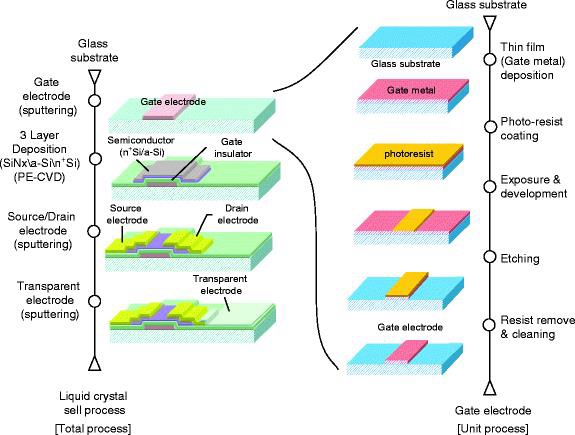
Function: Fabricate millions of Thin-Film Transistors (TFTs), scan lines, data lines and pixel ITO electrodes on glass, forming a switching matrix for the display panel.
Cyclic workflow: Thin-film Deposition → Photolithography → Etching → Stripping, repeated 5–7 times.
1. Substrate cleaning for ultra-thin alkali-free glass
2. Thin-film Deposition
◦ Sputtering: Metal gate layer
◦ PECVD: Silicon nitride insulation layer, amorphous silicon (a-Si) semiconductor layer, n+ doped silicon
◦ Sputtering: Source/drain metal layers, ITO transparent pixel electrodes
3. Photolithography
Photoresist coating → Pre-baking → UV exposure with photomask → Development
4. Etching: Dry etching / Wet etching to form circuit patterns
5. Stripping and cleaning
6. Array electrical testing, laser repair for bright spots and open-circuit defects
Main technology types:
• a-Si (Amorphous Silicon) TFT: Widely adopted for industrial displays and POS screens with moderate cost.
• LTPS (Low-Temperature Polycrystalline Silicon): Used for mobile phones and high-end notebook panels featuring higher resolution and faster response speed.
2. Color Filter (CF) Substrate Process
Function: Fabricate RGB color layers on the second glass substrate to realize color display.
1. Glass substrate cleaning
2. Black Matrix (BM): Shade gaps between pixels to prevent light leakage and improve contrast ratio
3. Sequential formation of R (Red) / G (Green) / B (Blue) sub-pixels via repeated photolithography
4. Over Coat (OC): Protective layer for surface planarization
5. Photo Spacer (PS): Support two glass substrates to maintain uniform cell gap of 3–5 μm
6. Sputter deposition of ITO common electrode (COM)
7. Optical visual inspection
3. Cell Assembly Process (Bond Array and CF into liquid crystal cell)
1. PI (Polyimide) alignment layer coating, baking and curing
2. Rubbing treatment: Generate consistent pre-tilt angle for liquid crystal molecules
3. Dust removal cleaning
4. Sealant dispensing on substrate edges (liquid crystal injection port reserved)
5. High-precision vacuum alignment and lamination of Array and CF substrates
6. Liquid crystal filling
◦ Traditional method: Vacuum capillary injection
◦ Modern ODF (One Drop Fill): Dispense liquid crystal before lamination with higher productivity
7. End-sealing, UV & thermal curing of sealant
8. Cutting large mother glass into single panels, edge grinding and cleaning
9. Polarizer lamination (front & rear orthogonal polarizers)
10. Cell lighting test for bright dots, dark dots, Mura and uneven color
The finished product at this stage is called Cell panel, which cannot light up independently without driver IC and backlight.
4. Module Assembly Process (LCM)
Final product = LCD Cell + driving circuit + Backlight Unit (BLU) + FPC + mechanical frames
1. Panel cleaning, pre-lamination of ACF conductive adhesive
2. COG bonding: Thermally press driver IC directly onto glass edge (mainstream for industrial TFT screens)
Alternative: COF (Chip on Film) for high-end narrow-border products
3. Hot-press bonding of FPC flexible cable
4. Backlight Unit assembly: LED strips + Light Guide Plate (LGP) + Diffuser sheets + Brightness Enhancement Films + Reflector sheet
5. Assembly of metal/plastic frame
6. High-temperature aging test to expose early failures
7. Full function inspection: brightness, contrast, color gamut, interface performance, viewing angle
8. Final visual inspection, cleaning and packaging
For capacitive touch TFT displays, extra TP touch layer lamination process (GFF / OGS solutions) is required.
Glossary for technical communication
1. Cell Gap: Gap between Array and CF substrates, determining liquid crystal response speed
2. ODF: One Drop Fill liquid crystal dispensing process
3. ACF: Anisotropic Conductive Film; conductive vertically while insulated horizontally, critical material for IC bonding
4. Mura: Uneven brightness or cloud-like stain, one of the most common panel defects
5. Polarizer: Polarizing film; LCD cannot control light transmission without polarizers